MCQs for Physics Class 12 with Answers Chapter 14 Semiconductor Electronics Materials Devices and Simple Circuits
Students of class 12 Physics should refer to MCQ Questions Class 12 Physics Semiconductor Electronics: Materials, Devices and Simple Circuits with answers provided here which is an important chapter in Class 12 Physics NCERT textbook. These MCQ for Class 12 Physics with Answers have been prepared based on the latest CBSE and NCERT syllabus and examination guidelines for Class 12 Physics. The following MCQs can help you to practice and get better marks in the upcoming class 12 Physics examination
Chapter 14 Semiconductor Electronics: Materials, Devices and Simple Circuits MCQ with Answers Class 12 Physics
MCQ Questions Class 12 Physics Semiconductor Electronics: Materials, Devices and Simple Circuits provided below have been prepared by expert teachers of grade 12. These objective questions with solutions are expected to come in the upcoming Standard 12 examinations. Learn the below provided MCQ questions to get better marks in examinations.
Question. Choose the only false statement from the following.
(a) In conductors, the valence and conduction bands may overlap.
(b) Substances with energy gap of the order of 10 eV are insulators.
(c) The resistivity of a semiconductor increases with increase in temperature.
(d) The conductivity of a semiconductor increases with increase in temperature.
Answer
C
Question. Application of a forward bias to a p–n junction
(a) widens the depletion zone.
(b) increases the potential difference across the depletion zone
(c) increases the number of donors on the n side.
(d) increases the electric field in the depletion zone.
Answer
C
Question. A transistor has three impurity regions. All the three regions have different doping levels. In order of increasing doping level, the regions are
(a) emitter, base and collector
(b) collector, base and emitter
(c) base, emitter and collector
(d) base, collector and emitter
Answer
D
Question. In a junction diode, the holes are due to
(a) protons
(b) extra electrons
(c) neutrons
(d) missing electrons
Answer
D
Question. By increasing the temperature, the specific resistance of a conductor and a semiconductor
(a) increases for both
(b) decreases for both
(c) increases, decreases
(d) decreases, increases
Answer
C
Question. The energy band gap is maximum in
(a) metals
(b) superconductors
(c) insulators
(d) semiconductors.
Answer
C
Question. When n-P-n transistor is used as an amplifier, then
(a) electrons move from collector to emitter
(b) electrons move from emitter to collector
(c) electrons move from collector to base
(d) holes move from emitter to collector
Answer
B
Question. An oscillator is nothing but an amplifier with
(a) positive feedback
(b) large gain
(c) no feedback
(d) negative feedback
Answer
A
Question. The intrinsic semi conductor becomes an insulator at
(a) 0ºC
(b) 0 K
(c) 300 K
(d) –100ºC
Answer
B
Question. NAND and NOR gates are called universal gates primarily because they
(a) are available universally
(b) can be combined to produce OR, AND and NOT gates
(c) are widely used in Integrated circuit packages
(d) are easiest to manufacture
Answer
B
Question. The device that can act as a complete electronic circuit is
(a) junction diode
(b) integrated circuit
(c) junction transistor
(d) zener diode
Answer
B
Question. The ratio of electron and hole currents in a semiconductor is 7/4 and the ratio of drift velocities of electrons and holes is 5/4, then the ratio of concentrations of electrons and holes will be
(a) 5/7
(b) 7/5
(c) 25/49
(d) 49/25
Answer
B
Question. If the forward voltage in a semiconductor diode is changed from 0.5V to 0.7 V, then the forward current changes by 1.0 mA. The forward resistance of diode junction will be
(a) 100 Ω
(b) 120 Ω
(c) 200 Ω
(d) 240 Ω
Answer
C
Question. A transistor has β = 40. A change in base current of 100 m A, produces change in collector current
(a) 40 × 100 microampere
(b) (100 – 40) microampere
(c) (100 + 40) microampere
(d) 100/40 microampere
Answer
A
Question. In a common emitter transistor amplifier β = 60, Ro = 5000 W and internal resistance of a transistor is 500 Ω. The voltage amplification of amplifier will be
(a) 500
(b) 460
(c) 600
(d) 560
Answer
C
Question. The current gain in transistor in common base mode is 0.99. To change the emitter current by 5 mA, the necessary change in collector will be
(a) 0.196 mA
(b) 2.45 mA
(c) 4.95 mA
(d) 5.1 mA
Answer
C
Question. What is the voltage gain in a common emitter amplifier, where input resistance is 3 Ω and load resistance 24 Ω, β = 0.6 ?
(a) 8 . 4
(b) 4 . 8
(c) 2 . 4
(d) 480
Answer
B
Question. In common emitter amplifier the Ic/Ie is 0.98. The current gain will be
(a) 4.9
(b) 7.8
(c) 49
(d) 78
Answer
C
Question. In the diagram, the input is across the terminals A and C and the output is across B and D. Then the output is
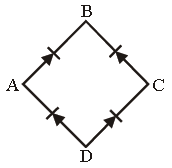
(a) zero
(b) same as the input
(c) full wave rectifier
(d) half wave rectifier
Answer
C
Question. In the following circuit, the output Y for all possible inputs A and B is expressed by the truth table.

(a) A B Y
0 0 1
0 1 1
1 0 1
1 1 0
(b) A B Y
0 0 1
0 1 0
1 0 0
1 1 0
(c) A B Y
0 0 0
0 1 1
1 0 1
1 1 1
(d) A B Y
0 0 0
0 1 0
1 0 0
1 1 1
Answer
C
Question. In the case of a common emitter transistor amplifier the ratio of the collector current to the emitter current Ic /Ie is 0.96. The current gain of the amplifier is
(a) 6
(b) 48
(c) 24
(d) 12
Answer
C
Question. Barrier potential of a P-N junction diode does not depend on
(a) doping density
(b) diode design
(c) temperature
(d) forward bias
Answer
B
Question. In semiconductors at a room temperature
(a) the conduction band is completely empty
(b) the valence band is partially empty and the conduction band is partially filled
(c) the valence band is completely filled and the conduction band is partially filled
(d) the valence band is completely filled
Answer
C
Question. Of the diodes shown in the following diagrams, which one is reverse biased ?

Answer
D
Question. Choose the only false statement from the following.
(a) In conductors the valence and conduction bands may overlap.
(b) Substances with energy gap of the order of 10 eV are insulators.
(c) The resistivity of a semiconductor increases with increase in temperature.
(d) The conductivity of a semiconductor increases with increase in temperature.
Answer
C
Question. For transistor action
(1) Base, emitter and collector regions should have similar size and doping concentrations.
(2) The base region must be very thin and lightly doped.
(3) The eimtter-base junction is forward biased and base collector junction is reverse based.
(4) Both the emitter-base junction as well as the base collector junction are forward biased.
(a) (3) and (4)
(b) (4) and (1)
(c) (1) and (2)
(d) (2) and (3)
Answer
D
Question. The following figure shows a logic gate circuit with two inputs A and B and the output Y. The voltage waveforms of A, B and Y are given
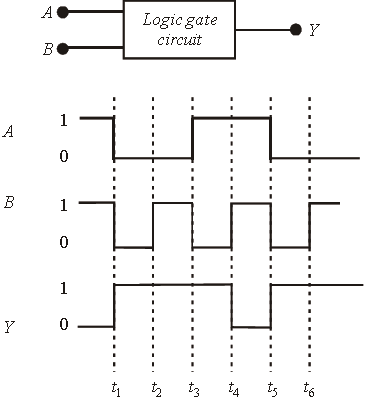
The logic gate is :
(a) NAND gate
(b) NOR gate
(c) OR gate
(d) AND gate
Answer
A
Question. Symbolic representation of four logic gate are shown as Pick out which ones are for AND, NAND and NOT gates, respectively
(a) (ii), (iii) and (iv)
(b) (iii), (ii) and (i)
(c) (iii), (iii) and (iv)
(d) (ii), (iv) and (iii)
Answer
D
Question. Pure Si at 500K has equal number of electron (ne) and hole (nh) concentrations of 1.5 × 10¹⁶ m–3. Doping by indium increases nh to 4.5 × 10²² m–3. The doped semiconductor is of
(a) n–type with electron concentration
ne = 5 × 10²² m–3
(b) p–type with electron concentration
ne = 2.5 ×10¹⁰ m–3
(c) n–type with electron concentration
ne = 2.5 × 10²³ m–3
(d) p–type having electron concentration
ne = 5 × 10⁹ m–3
Answer
D
Question. A zener diode, having breakdown voltage equal to 15V, is used in a voltage regulator circuit shown in figure. The current through the diode is
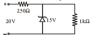
(a) 10 mA
(b) 15 mA
(c) 20 mA
(d) 5 mA
Answer
D
Question. The input resistance of a silicon transistor is 100 W. Base current is changed by 40 mA which results in a change in collector current by 2 mA. This transistor is used as a common emitter amplifier with a load resistance of 4 KW. The voltage gain of the amplifier is
(a) 2000
(b) 3000
(c) 4000
(d) 1000
Answer
A
Question. In a common emitter (CE) amplifier having a voltage gain G, the transistor used has transconductance 0.03 mho and current gain 25. If the above transistor is replaced with another one with transconductance 0.02 mho and current gain 20, the voltage gain will be
(a) 1.5 G
(b) (1/5) G
(c) (5/4) G
(d) (2/3) G
Answer
D
Question. An oscillator is nothing but an amplifier with
(a) positive feedback
(b) large gain
(c) no feedback
(d) negative feedback
Answer
A
Question. In an unbiased p-n junction, holes diffuse from the p-region to n-region because of
(a) the potential difference across the p-n junction
(b) the attraction of free electrons of n-region
(c) the higher hole concentration in p-region than that in n-region
(d) the higher concentration of electrons in the n-region than that in the p-region
Answer
C
Question. One way in which the operation of a n-p-n transistor differs from that of a p-n-p
(a) the emitter junction is reversed biased in n-p-n
(b) the emitter junction injects minority carriers into the base region of the p-n-p
(c) the emitter injects holes into the base of the p-n-p and electrons into the base region of n-p-n
(d) the emitter injects holes into the base of n-p-n
Answer
C
Question. A TV tower has a height of 100 m. How much population is covered by the TV broadcast if the average population density around the tower is 1000 km–2 ? (radius of the earth = 6.37 × 10⁶ m)
(a) 4 lakh
(b) 4 billion
(c) 40,000
(d) 40 lakh
Answer
D
Question. The ratio of forward biased to reverse biased resistance for pn junction diode is
(a) 10–1 : 1
(b) 10–2 : 1
(c) 104 : 1
(d) 10–4 : 1
Answer
D
Question. In figure given below V0 is the potential barrier across a p–n junction, when no battary is connected across the junction
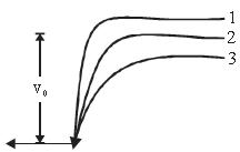
(a) 1 and 3 both correspond to forward bias of junction
(b) 3 corresponds to forward bias of junction and 1 corresponds to reverse bias of junctions
(c) 1 corresponds to forward bias and 3 corresponds to reverse bias of junction
(d) 3 and 1 both correspond to reverse bias of junction
Answer
B
Question. In figure given below, assuming the diodes to be ideal
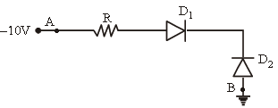
(a) D1 is forward biased and D2 is reverse biased and hence current flows from A to B
(b) D2 is forward biased and D1 is reverse biased and hence no current flows from B to A and vice–versa
(c) D1 and D2 are both forward biased and hence current flows from A to B
(d) D1 and D2 are both reverse biased and hence no current flows from A to B and vice – versa
Answer
B
Question. A 220 V AC supply is connected between points A and B (figure). What will be the potential difference V across the capacitor?

(a) 220 V
(b) 110 V
(c) 0 V
(d) 220 √2V
Answer
D
Question. Truth table for the given circuit is

(a) A B E
0 0 1
0 1 0
1 0 1
1 1 0
(b) A B E
0 0 1
0 1 0
1 0 0
1 1 0
(c) A B E
0 0 0
0 1 1
1 0 0
1 1 1
(d) A B E
0 0 0
0 1 1
1 0 1
1 1 0
Answer
C
Question. The output(X) of the logic circuit shown in figure will be
Answer
B
Question. The given graph represents V – I characteristic for a semiconductor device.
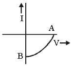
Which of the following statement is correct ?
(a) It is V – I characteristic for solar cell where, point A represents open circuit voltage and point B short circuit current.
(b) It is a for a solar cell and point A and B represent open circuit voltage and current, respectively.
(c) It is for a photodiode and points A and B represent open circuit voltage and current, respectively.
(d) It is for a LED and points A and B represent open circuit voltage and short circuit current, respectively.
Answer
A
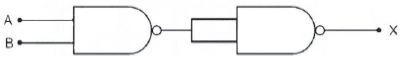
Question. Which logic gate is represented by the following combination of logic gate ?

(a) NAND
(b) AND
(c) NOR
(d) OR
Answer
B
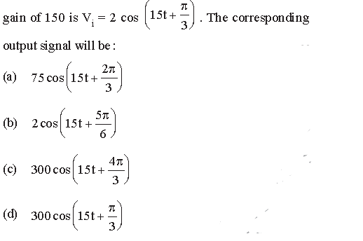
Question. The input signal given to a CE amplifier having a voltage
Answer
C
Question. In a common emitter transistor amplifier the audio signal voltage across the collector is 3V. The resistance of collector is 3 kW. If current gain is 100 and the base resistance is 2 kW, the voltage and power gain of the amplifier is
(a) 15 and 200
(b) 150 and 15000
(c) 20 and 2000
(d) 200 and 1000
Answer
B
Question. Which one of the following represents forward bias diode?

Answer
D
Question. The barrier potential of a p-n junction depends on:
(A) type of semi conductor material
(B) amount of doping
(C) temperature
Which one of the following is correct ?
(a) (A) and
(B) only (b) (B) only
(c) (B) and (C) only
(d) (A), (B) and (C)
Answer
D
Question. In a common emitter (CE) amplifier having a voltage gain G, the transistor used has transconductance 0.03 mho and current gain 25. If the above transistor is replaced with another one with transconductance 0.02 mho and current gain 20, the voltage gain will be
(a) 1.5
(b) (1/3) G
(c) (1/4) G
(d) (2/3) G
Answer
D
Question. The output of the given circuit in figure given below

(a) would be zero at all times
(b) would be like a half wave rectifier with positive cycles in output
(c) would be like a half wave rectifier with negative cycles in output
(d) would be like that of a full wave rectifier
Answer
C
