Sample Paper Class 12 Physics
Get Class 12 Physics Sample Papers free pdf download which is based on the latest pattern of CBSE and NCERT. It involves every one of the points given in NCERT class 12 Physics book. You can easily download sample paper accounts class 12 is given below.
Download 12th Physics Question paper in PDF free of charge. It will help you to make your preparation better to score higher marks in exams. These Class 12 Physics Sample Papers PDFs are prepared by our expert teacher.
This 12th Physics Question Paper PDF assists you with revising the complete chapter in minutes. One of the best tips suggested by teachers is Solving the sample papers during exam time.
We bring here the latest collection of Sample Papers for Class 12 Physics prepared as per the latest examination pattern issued by CBSE. Students can refer to the latest paper below available with answers and also download the suggested guess papers in PDF format for free. Students should solve the papers in exam type environment at home and then compare their results with the answers provided below. Students should regularly solve questions given in DK Goel Class 12 book and also solve the papers given below
Sample Paper Class 12 Physics Term 1 Set A
Section-A
1. A semiconductor has equal electron and hole concentration of 2 × 10⁸ m–3, concentration increases to 4 × 10¹⁰ m–3.
(i) What type of semiconductor is obtained on doping? (ii) Calculate the new electron hole concentration of the semiconductor. (iii) How does the energy gap vary with doping?
Answer. ni = 2 × 10⁸ m–3
On doping nh = 4 × 10¹⁰ m–3
(i) As on doping the number density of holes have increased so it is a p-type semiconductor.
(ii) ni2 = nenh
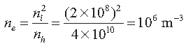
(iii) Energy gap decreases with doping due to the creation of acceptor energy level.
2. The energy levels of an atom are shown in figure. Which transition corresponds to emission of radiation of (i) maximum wavelength (ii) minimum wavelength?

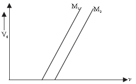
Figure shows variation of stopping potential (V0) with frequency (v) for two photosensitive material M1 and M2.
(i) Why is the slope same for both lines?
(ii) For which material will the emitted electrons have greater kinetic energy for the incident radiations of the same frequency? Justify your answer.
Answer. For transition A, Energy of emitted photon = 0 – (– 2) = 2 eV
For transition B, Energy of emitted photon = 0 – ( – 4.5) = 4.5 eV
For transition C, Energy of emitted photon = – 2 – (– 4.5) = 2.5 eV
For transition D, Energy of emitted photon = – 2 – (– 10) = 8 eV
Therefore, for maximum wavelength, E should be minimum. Transition A for which energy difference E is minimum corresponds to emission of radiation of max. wavelength.
Similarly, transition D for which energy diff. E is minimum, corresponds to emission of radiation of minimum wavelength.
OR
(i) From Einstein’s photoelectric equation
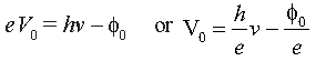
The slope of stopping potential vs frequency graph is a constant equal to h/e, and h/e in same for all metals. So the slope is same for both lines.
(ii) As (K.E.)max = hv – hv0
For metal M1, the threshold frequency v0 is lesser. So the (K.E.)max is larger for metal M1 so metal M1 will emit photoelectrons of higher K.E.
3. In V-I characteristics of a p-n junction diode:
(a) Why is the current under reverse bias almost independent of the applied potential upto a critical voltage?
(b) Why does the reverse current show a sudden increase at critical voltage?
Answer. (a) When a p-n junction is reverse biased, the minority charge carriers i.e., electrons from p side and holes from n side drift towards the junction. The number density of minority charge carrier remains almost constant upto a critical voltage. So the current under the reverse bias is independent of applied voltage upto a critical voltage.
(b) When the reverse biased voltage is increased beyond critical voltage, the electric field at the junction becomes sstrong enough to pull out electrons from the host atoms on p-side and accelerates them towards n-side. Due to the movement of these electrons across the junction, the current increases suddenly at critical voltage.
Section-B
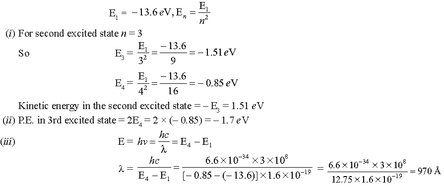
4. Ground state energy of hydrogen atom is – 13.6 eV
(i) What is the K.E. of an electron in the second excited state?
(ii) What is the P.E. of an electron in the third excited state?
(iii) If the electron jumps to the ground state from the third excited state, calculate the wavelength of the photon emitted.
E1 = −13.6 eV, En = E1/n2
Answer. (i) For second excited state n = 3
5. Describe briefly using the necessary circuit diagram, the three basic processes which take place to generate the emf in a solar cell when light falls on it. Draw the I-V characteristics of a solar cell.
Write two important criteria required for the selection of a material for solar cell fabrication.
Answer. The generation of emf by a solar cell when light falls on it is due to :
(i) Generation of e-h pairs due to light (with hv > Eg) close to the junction.
(ii) Separation: of electrons and holes due to electric field of the depletion region. Electrons are swept to n-side and holes to p-side.
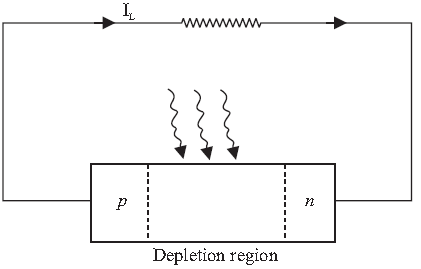
(iii) Collection : Electrons reaching n-side are collected by front contact and holes reaching p-side are collected by the back contact.
Thus p-side becomes +ve and n-side –ve giving rise to photo-voltage.
When an external load is connected, photo-current IL flows through the load.
V – I characteristics of solar cell is drawn in 4th quadrant because a solar cell does not draw current but
supplies it to the load.

Semiconductors with band gap close to 1.5 eV are ideal materials for solar cell fabrication. They are made with sesmiconductor like Si (Eg = 1.1 eV), Ga As (Eg = 1.43 eV), Cd Te (Eg = 1.45 eV), Cu In Se2 (Eg = 1.049 eV) etc.
Important criteria for selection of material:
(i) Band gap (~ 1.0 to 1.8 eV) (ii) High optical absorption (~ 104 cm–1)
(iii) Electrical conductivity (iv) Availability of raw material
(v) Cost.
6. Explain the concept of nuclear forces. Discuss their characteristic properties. Which properties distinguish them from electrostatic forces?
Answer. Nuclear force : Inside the nucleus large number of protons are held along with the neutrons in a very small space.
The Coulombian force of repulsion between protons (due to like charges) is nullified by a strong attractive force called nuclear force.
So Nuclear forces are the strong forces of attraction which hold together the nucleus in a small space called nucleus, inspite of strong electrostatic force of repulsion between protons.
Characteristic/properties of nuclear forces:
Refer theory topic no. 1 under the heading Nuclear force.
Comparison between electrostatic and nuclear force:

7. (a) State two important features of Einstein’s photoelectric equation.
(b) Radiation of frequency 1015 Hz is incident on two photosensitive surface P and Q. There is no photoemission from surface P. Photoemission occurs from surface Q but photoelectrons have zero kinetic energy. Explain these observations and find the value of work function for surface Q.
Answer. (a) According to Einstein’s photoelectric equation (KE)max = hn – hn0
(i) If frequency of incident photon n is less than the threshold freq. n0, no emission of photo-electrons is possible because for n < n0
(KE)max is negative, which is not possible
(ii) With increase in frequency of incident radiation there will be increase in (KE) of photoelectrons but no change in photo-electric current.
(b) n = 1015 Hz
As there in no photoemission from surface P, so threshold freq. of P is more than 1015 Hz
For metal Q, (KE) = 0
So hn = f0 + KE
∴ hn = f0
Work function of Q = hn = 6.6 × 10–34 × 1015 = 6.6 × 10⁻¹⁹ J

8. A compound microscope uses an objective lens of focal length 4 cm and eyepiece lens of focal length 10 cm. An object is placed at 6 cm from the objective lens. Calculate the magnifying power of the compound microscope.
Also calculate the length of the microscope.
OR
An optical instrument uses eye-lens of power 12.5 D and objective lens of power 50 D and has a tube length of 20 cm. Name the optical instrument and calculate its magnifying power, if it forms the final image at infinity.
Answer. fo = 4 cm, fe = 10 cm, uo = – 6 cm, m = ?


9. In Young’s double slit experiment, explain with reason in each case, how the interference pattern changes, when
(i) Width of the slits is doubled
(ii) Separation between the slits is increased, and
(iii) Screen is moved away from the plane slits.
Answer. The fringe width β = Dλ/d
(i) When the width of the slit is doubled; the intensity of interfering wave becomes four times, intensity of maxima becomes 16 times i.e., fringes become brighter.
(ii) β ∝1/d , when separation between the slits is increased the fringe width decreases i.e., fringes comes closer.
(iii) b ∝ D, when screen is moved away from the plane of the slits, the fringe width increases i.e., fringes become farther away.
10. The following table gives data about the single slit diffraction experiment:
Wavelength of light Half angular width of the principal maxima
λ θ
pλ qθ
Find the ratio of the width of the slits used in the two cases. Would the ratio of the half angular width of the first secondary maxima, in the two cases, be also equal to q?
Answer. Let the slit width be a1 and a2 in the two cases

11. Why are infra-red radiations referred to as heat waves? Name the radiations which are next to these radiations in the electromagnetic spectrum having (i) shorter wavelength (ii) longer wavelength.
OR
Name the em waves in the wavelength range 10 nm to 10–3 nm. How are these waves generated? Write their two applications.
Answer. Infrared rays are produced by hot bodies or by vibrations of molecules or atoms.
IR rays are referred to as heat waves because they get easily absorbed by water molecules in most materials. Due to the increased thermal agitation their temperature increases and hence get heated. They are used in muscular pain relief.
(i) EM waves hav.ing short wavelength than infrared waves are visible, UV, X-rays and g-rays.
(ii) EM waves having longer wavelength than infrared waves are microwaves, short radio waves, television and FM radio.
OR
Em waves in the wavelength range 10 nm to 10–3 nm are X-ray. X-rays are generating by bombarding a metal target with high frequency electrons.
Uses:
(i) Diagnosis of bone fractures (ii) Treatment of some forms of cancer
Section-C
12. When the light from a monochromatic source is incident on a single monochromatic slit, it gets diffracted and a pattern of alternate bright and dark fringes is obtained on screen, called diffraction pattern of single slit. In diffraction pattern of single slit, it is found that.
(i) Central bright fringe is of maximum intensity and the intensity of any secondary bright fringe decreases with increase in its order.
(ii) Central bright fringe is twice as wide as any other secondary bright or dark fringe.
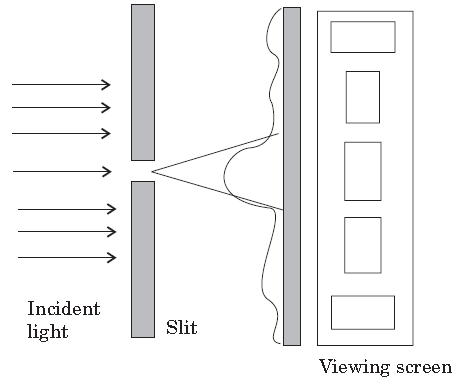
Based on the above facts, answer the following questions.
(i) A single slit of width 0.1 mm is illuminated by a parallel beam of light of wavelength 6000 Å and diffraction bands are observed on a screen 0.5 m from the slit. The distance of the third dark band from the central bright band is
(a) 3 mm
(b) 1.5 mm
(c) 9 mm
(d) 4.5 mm
Answer
A
(ii) In Fraunhofer diffraction pattern, slit width is 0.2 mm and screen is at 2 m away from the lens. If wavelength of light used is 5000 Å then the distance between the first minimum on either side the central maximum is
(a) 10–1 m
(b) 10–2 m
(c) 2 × 10⁻² m
(d) 2 × 10⁻¹ m
Answer
B
(iii) Light of wavelength 600 mm is incident normally on a slit of width 0.2 mm. The angular width of central maxima in the diffraction pattern is (measured from minimum to minimum)
(a) 6 × 10⁻³ rad
(b) 4 × 10⁻³ rad
(c) 2.4 × 10⁻³ rad
(d) 4.5 × 10⁻³ rad
Answer
A
(iv) A diffraction pattern is obtained by using a beam of red light. What will happen if the red light is replaced by the blue light?
(a) bands disappear
(b) bands become broader and farther apart
(c) no change will take place
(d) diffraction bands become narrower and crowded together
Answer
D
(v) To observe diffraction the size of obstacle
(a) should be λ/2where l is wavelength
(b) should be of the order of wavelength
(c) has no relation to wavelength
(d) should be much larger than the wavelength
Answer
B
